These are multi-layer PCBs in which layers are piled up one by one using laser technology and plating technology after forming a conductor pattern on an insulating layer. Because wiring is possible on the connection part of each layer, this method achieves higher density and higher integration than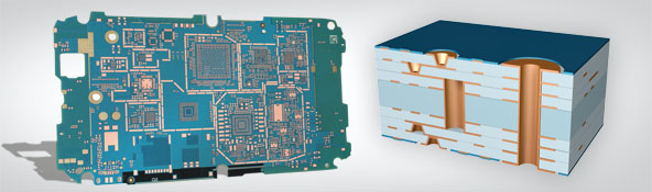 ordinary multi-layer through-hole PCBs. They are used for devices that require high-density wiring in a limited space.
These support the EMS business
Features
HDI PCBs with Staggered Via and Stacked Via
Any combination with Laser Via, IVH or Plated Through Hole is possible
Applications

Cross section

Stackup

Design rule


